Michael Keating et al.
[1] lists several low power techniques to tackle the dynamic and static
power consumption in modern SoC designs. Dynamic power control
techniques include clock gating, multi voltage, variable frequency, and
efficient circuits. Leakage power control techniques include power
gating, multi Vt cells. Common methods supported by EDA tools include
clock gating, gate sizing, low power placement, register clustering, low
power CTS, multi Vt optimization.
Some of the low power techniques in use today are listed in below table.
Different Low Power Techniques [3]
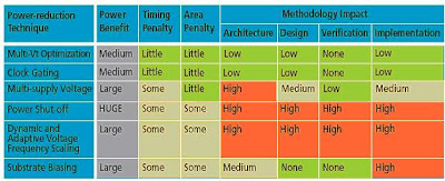
Trade-offs associated with the various power management techniques [2]
Above
table summarizes trade-offs associated with different power management
techniques. Power gating and DVFS demand large methodology change
whereas multi vt and clock gating affect least. Unless large leakage
optimization is not necessary it is always beneficial to go with either
multi vt or clock gating techniques. Based on the design complexity and
requirements combination of any low power techniques can be adopted.
Multi vt optimization along with the power gating is found to be
efficient in some of the complex designs. Advanced improvements in the
implementation (i.e. fabrication) technology has allowed substrate
biasing techniques to be used heavily as it does not pose any
architectural and design verification challenges and also provides high
leakage reduction.
References
[1] Michael Keating, David Flynn, Robert Aitken, Alan Gibsons and Kaijian Shi, “Low Power Methodology Manual for System on Chip Design”, Springer Publications, NewYork, 2007, www.lpmm-book.org, 4/9/2007
[2] Creating Low-Power Digital Integrated Circuits – The Implementation Phase, Cadence, 2007
[3]Godwin Maben, "Low Power Techniques in Use Today"

